Overview
A precision bidirectional current source designed from scratch — schematic, PCB, and firmware — for driving resistive-inductive loads with controlled current in both directions, smoothly crossing through zero. That zero-crossing capability is what makes it a true 4-quadrant converter. The target application is magnet power supply research at CERN, where you need to push current one way, pull it back, and do both accurately.
The power stage is a full H-bridge using four STP110N10F7 N-channel MOSFETs (100 V / 110 A), deliberately overspec'd for the ~4 A I'm targeting so the FETs run cool without heatsinks. The bridge switches at 100 kHz with center-aligned PWM off a 48 V bus. Current regulation runs on a TI C2000 F280049C executing a PI loop at the switching rate, reading current through an INA240A2 sense amplifier (50 V/V) on a 10 mΩ Kelvin-connected shunt in the load path. A hardware window comparator (MCP6567) provides a fast overcurrent trip at ±3 A that bypasses firmware entirely.
Power Stage
The H-bridge has two legs — Leg A (QH_A, QL_A) and Leg B (QH_B, QL_B) — with the load between their switch nodes. Differential duty-cycle control sets the net voltage across the load: both legs at 50% means zero volts, shifting them apart drives current one way or the other. A 220 µH inductor smooths the PWM into controlled DC current.
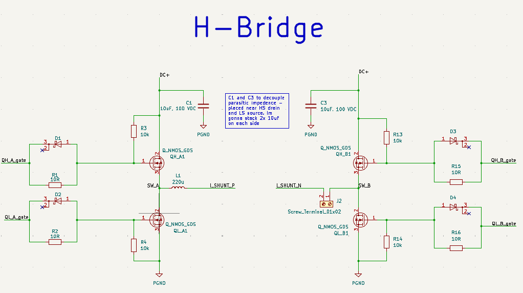
Each gate is driven through a 10 Ω series resistor with a BAT54A Schottky in anti-parallel — slow turn-on to limit dV/dt, fast turn-off to minimize the cross-conduction window during dead time. I verified the resistor power dissipation at 100 kHz: with Qg = 72 nC and 12 V drive, each gate resistor dissipates about 33 mW, well within the 125 mW rating of an 0805 package. The 10 kΩ pull-down resistors sit gate-to-source (not gate-to-drain, which was an earlier mistake I caught during review) to keep the FETs off when the driver tri-states.
Each leg has a pair of DC bus decoupling caps placed by priority: a 100 nF ceramic (C1, C4) with pads physically touching the high-side drain and low-side source copper to catch fast switching spikes, and a 10 µF ceramic (C2, C3) nearby for switching-frequency ripple current. This multi-tier decoupling approach is what keeps the voltage spikes on the DC bus manageable — no single cap can handle the full frequency range from DC to the switching transients.
Gate Drivers
Each half-bridge leg gets a UCC27211A driver that level-shifts the C2000's 3.3 V PWM up to 12 V for the MOSFET gates. The high-side uses bootstrap topology: a 1 µF cap charges through the UCC27211A's internal diode when the low-side is on, then floats up with the switch node. A 100 nF cap sits closer to the HB/HS pins than the bootstrap cap to handle the fast charge transients during gate switching.
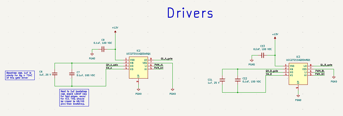
The VDD bypass caps (C9, C10) are 1 µF each — TI recommends 0.22–4.7 µF for this driver, and the original 0.1 µF was below the minimum. The integrated bootstrap diode saves an external Schottky per leg.
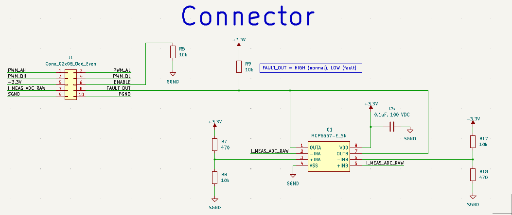
Current Sensing
The 10 mΩ shunt (2512 package, 1 W) sits in the load path between the switch nodes, not on the low-side return. This bidirectional placement means the INA240A2 sees actual load current in both polarities without common-mode headaches. The shunt uses a Kelvin connection in the PCB layout so the measurement isn't corrupted by voltage drops in the high-current copper.
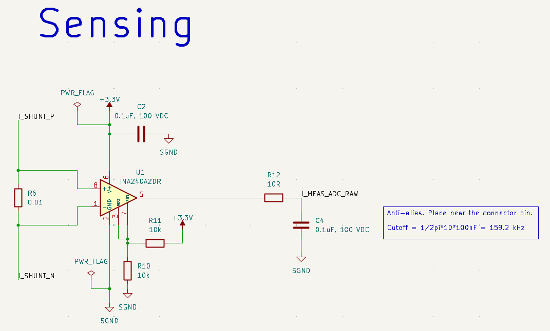
The INA240A2 outputs V = 50 × I × 0.01 + 1.65 V, giving a ±3.3 A full-scale range within the 0–3.3 V ADC window. At ±2 A operating current that uses counts 807–3289 out of the 12-bit ADC's 4096, giving 1.6 mA per count — far finer than the 2% accuracy target requires. An R-C anti-alias filter (10 Ω + 100 nF, fc ≈ 159 kHz) sits between the amplifier output and the ADC input, placed near the connector pin.
Hardware Overcurrent Protection
A MCP6567 dual comparator watches the INA240 output against two thresholds: a 10 kΩ / 470 Ω divider sets the upper trip at 3.15 V (+3.0 A) and the lower trip at 0.148 V (−3.0 A). Both comparators are open-drain, wired-AND into FAULT_OUT with a pull-up — if either threshold is crossed, FAULT_OUT drops and the C2000's trip-zone hardware kills all four PWM outputs. No firmware in that path. I used 1% resistors in the dividers because threshold accuracy directly determines how much usable current range you get before the protection fires.
Input Power & Indicators
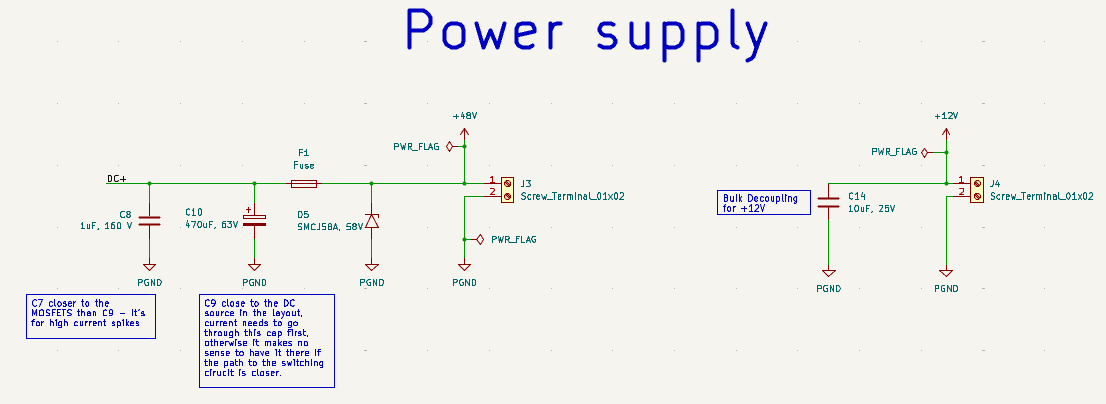
The 48 V bus enters through J1, passes through a 25 A mini blade fuse, and hits the DC rail. Bulk storage is a 470 µF / 100 V electrolytic (upgraded from 63 V to give proper margin against switching spikes on a 48 V bus) in parallel with a 1 µF / 160 V WIMA film cap for high-frequency transient current. A SMCJ58A TVS clamps spikes above ~64 V. The 12 V gate driver supply comes in on J2 with a 10 µF bulk cap.
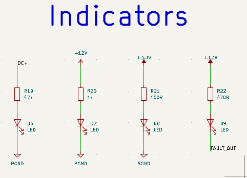
Four indicator LEDs give immediate visual status without a multimeter: green for 48 V present (post-fuse, so it also confirms the fuse is intact), yellow for 12 V driver supply, red for 3.3 V logic rail, and a second red that lights when FAULT_OUT goes low. The 48 V indicator uses a 47 kΩ series resistor to keep dissipation under 50 mW — a common mistake is using a standard 330 Ω LED resistor at 48 V, which would dissipate over 6 W and burn.
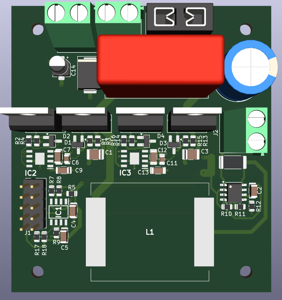
PCB Layout
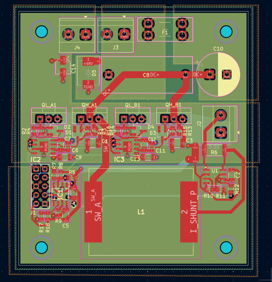
Four layers: top copper for components and power routing, inner layer 1 as solid PGND plane, inner layer 2 split between +48 V, +12 V and +3.3V power, bottom copper for signals and sense traces. The layout follows a three-zone strategy — power stage at top, drivers in the middle, sensing and connector at the bottom — with PGND and SGND connecting at a single star point near the shunt.
Ten test points are placed for oscilloscope access during bring-up: SW_A and SW_B within 5 mm of their FETs (longer probe leads would add parasitic inductance and make the ringing look worse than reality), both gate signals for dead-time verification, the INA240 output, DC+, FAULT_OUT, the raw shunt voltage, and separate PGND/SGND ground clips. The ground clip placement matters — probing a switching node with the ground clipped to SGND instead of PGND injects noise into the measurement that isn't actually there.
Controller Interface
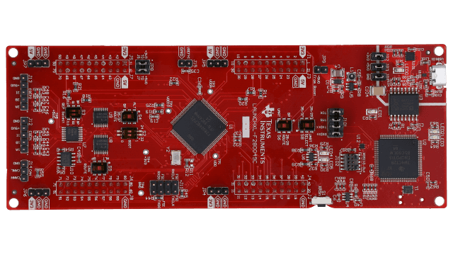
The C2000 LaunchPad connects through a 2×5 header carrying four PWM signals, the analog current measurement, enable, FAULT_OUT, power, and both ground domains. The +3.3 V pin sits between the PWM lines and I_MEAS_ADC_RAW, acting as a quiet buffer so the analog path doesn't pick up switching noise from the adjacent PWM traces. FAULT_OUT has a pull-up to 3.3 V — high means normal, low means the hardware comparator tripped.
| Pin 1 | PWM_AH | Pin 2 | PWM_AL |
| Pin 3 | PWM_BH | Pin 4 | PWM_BL |
| Pin 5 | +3.3V | Pin 6 | ENABLE |
| Pin 7 | I_MEAS_ADC_RAW | Pin 8 | FAULT_OUT |
| Pin 9 | SGND | Pin 10 | PGND |
Bring-Up & Testing
I wrote a 10-phase bring-up procedure before the boards arrived, working through it on paper so I wouldn't be improvising with 48 V on the bench. The sequence is designed around one principle: never test two unknowns at once. Each phase isolates a single subsystem.
Phases 1–3 happen with no bus voltage at all — visual inspection, continuity checks, then powering the 12 V and 3.3 V rails to verify the gate drivers and sensing chain are alive. Phase 4 runs the PWM into unbiased FETs (no bus = no switching current = safe) to confirm dead time and complementary operation on the scope. Phase 5 injects a small test current through the shunt to validate the INA240 gain and ADC scaling before any real power flows.
Only in Phase 6 does bus voltage appear, starting at 12 V with a 0.5 A current limit. The voltage ramp-up is strictly 12 V → 24 V → 48 V with re-testing at each step. Phase 7 closes the current loop at low voltage, Phase 8 ramps to full voltage, and Phase 9 captures the three KPIs: regulation accuracy (< 2%), step settling time (< 10 ms), and a clean bipolar sweep through zero.
References
Jason Sachs, “Lost Secrets of the H-Bridge, Part IV: DC Link Decoupling” — the best explanation I found on why a single decoupling cap is never enough and how to think about multi-tier decoupling in switching bridges.
PCBWay, “Powerful H-Bridge DC Motor Driver” — a practical reference design that informed some of the layout decisions, particularly the FET placement and power loop geometry.
Texas Instruments, UCC27211A datasheet, INA240 datasheet — all relevant datasheets are kept in a /datasheets folder in the project repository.
Full schematic: 4Q_Current_Source_schematics.pdf